- 您现在的位置:买卖IC网 > Sheet目录1990 > BQ4285EP (Texas Instruments)IC RTC W/114X8 NVSRAM 24-DIP
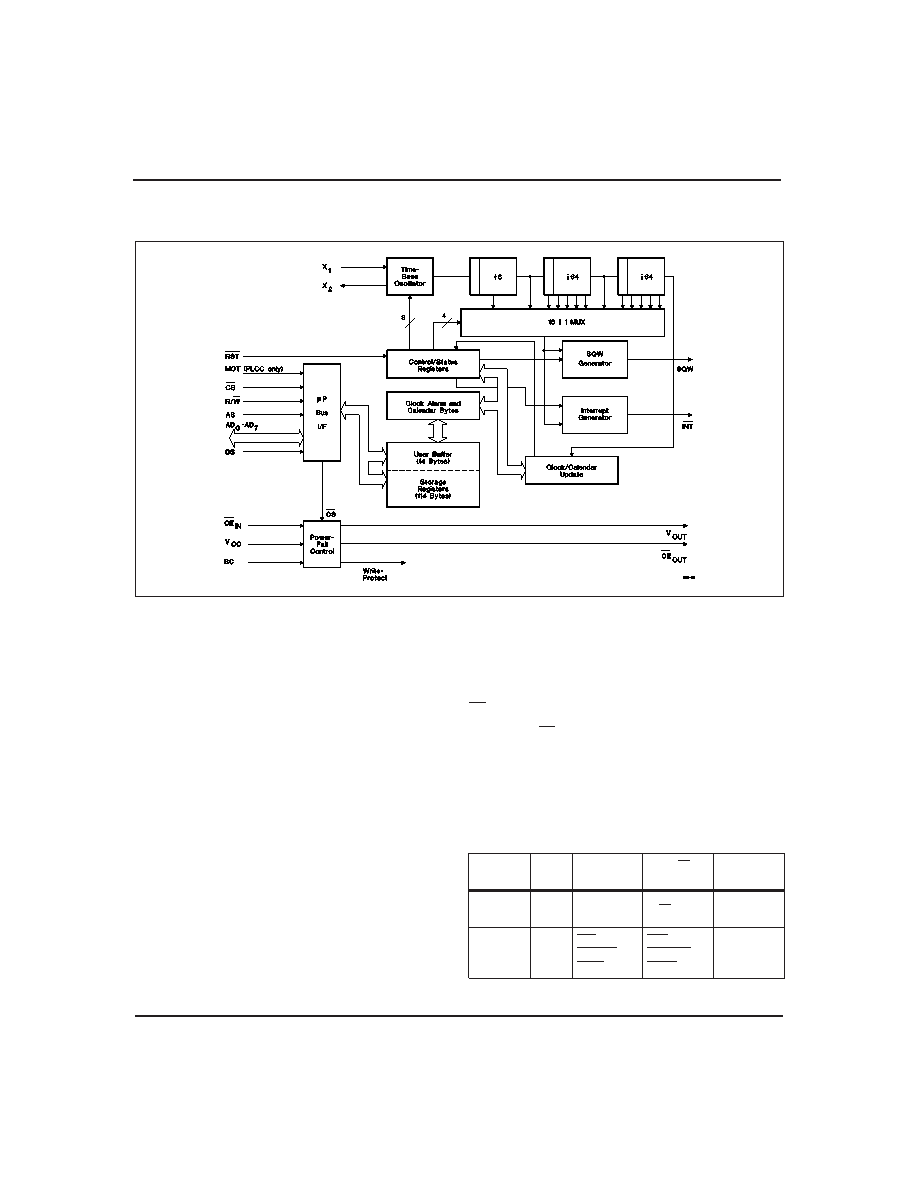
Block Diagram
standard CMOS SRAM nonvolatile during power-fail
conditions. During power-fail, the bq4285E/L auto-
matically write-protects the external SRAM and pro-
vides a VCC output sourced from the clock backup
battery.
Pin Descriptions
AD0–AD7
Multiplexed address/data input/
output
The bq4285E/L bus cycle consists of two
phases: the address phase and the data-
transfer phase. The address phase precedes
the data-transfer phase.
During the ad-
dress phase, an address placed on AD0–AD7
is latched into the bq4285E/L on the falling
edge of the AS signal.
During the data-
transfer phase of the bus cycle, the AD0–AD7
pins serve as a bidirectional data bus.
MOT
Connect to VSS for normal operation
The setting should not be changed during
system operation. MOT is internally pulled
low by a 20K
resistor. For the DIP and
SOIC packages, this pin is internally con-
nected to VSS, enabling the bus timing for
the Intel architecture.
CS
Chip select input
CS should be driven low and held stable
during the data-transfer phase of a bus cy-
cle accessing the bq4285E/L.
2
Bus
Type
MOT
Level
DS
Equivalent
R/W
Equivalent
AS
Equivalent
Intel
VSS
RD,
MEMR, or
I/OR
WR,
MEMW, or
I/OW
ALE
Table 1. Bus Setup
bq4285E/L
发布紧急采购,3分钟左右您将得到回复。
相关PDF资料
BQ4847YMT
IC RTC W/NVSRAM CONTROL T-MOD
BU2280FV-E2
IC CLOCK GEN DVD-VIDEO SSOP-B24
BU2363FV-E2
IC CLOCK GEN DVD-VIDEO SSOP-B16
BU2365FV-E2
IC CLOCK GEN W/VCXO SSOP-B24
BU2505FV-E2
IC DAC 10BIT 10-CHAN SSOP-B20
BU2508FV-E2
IC DAC 10BIT 4-CHAN SSOP14
BU3076HFV-TR
IC CLOCK GEN 1CH HVSOF6
CA3338AMZ96
IC DAC 8BIT 50MSPS R-R 16-SOIC
相关代理商/技术参数
BQ4285ES
制造商:未知厂家 制造商全称:未知厂家 功能描述:
BQ4285L
制造商:未知厂家 制造商全称:未知厂家 功能描述:Enhanced RTC With NVRAM Control
BQ4285LP
制造商:TI 制造商全称:Texas Instruments 功能描述:Enhanced RTC With NVRAM Control
BQ4285LQ
制造商:未知厂家 制造商全称:未知厂家 功能描述:
BQ4285LS
制造商:Rochester Electronics LLC 功能描述:- Bulk
BQ4285LSTR
制造商:TI 制造商全称:Texas Instruments 功能描述:Enhanced RTC With NVRAM Control
BQ4285P-
制造商:TI 制造商全称:Texas Instruments 功能描述:Real-Time Clock RTC With NVRAM Control
BQ4285P-SB2
功能描述:实时时钟 RTC IC: 114x8 NVSRAM & NVSRAM Control RoHS:否 制造商:Microchip Technology 功能:Clock, Calendar. Alarm RTC 总线接口:I2C 日期格式:DW:DM:M:Y 时间格式:HH:MM:SS RTC 存储容量:64 B 电源电压-最大:5.5 V 电源电压-最小:1.8 V 最大工作温度:+ 85 C 最小工作温度: 安装风格:Through Hole 封装 / 箱体:PDIP-8 封装:Tube